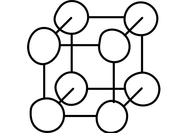
Light absorption
When light penetrates the semiconductor, it starts the process of exchanging energy with crystalline lattice. Let us determine I as a light intensity. Part of light flow is reflected from a surface of a crystal.
Light, going through the semiconductor is weakening. Let us consider a thin layer of a semiconductor dx. Then the quantity of light dI, is absorbed by the layer dx:dI = αIdx. Energy is decreasing. α is an absorption coefficient, it characterises change of light in the unit of length of a semiconductor. For the light intensity we have the formula, Buger-Lambert’s Law:
I(x) = I1exp (-αx), where I1 = I0(1 – R) – light, going through the semiconductor’s surface.
At the normal incidents of the light rays on the semiconductor, the absorption coefficient can be found by the formula:
, where n is a refractive index of a material.
Dependence of absorption coefficient from wavelength and photons energy is called the spectrum of compound absorption. Irradiation absorption in a semiconductor can be related to the change of state of free or bound electrons, and also to the change of oscillation energy of lattice atoms. Semiconductors have several mechanisms of optical absorption, and every mechanism corresponds to some exact part of an absorption spectrum.
Intrinsic absorption is due to transition of charge careers from the valence band to conductance band, i.e. quantity of energy waste for semiconductor atom ionisation (Figure 17). Intrinsic absorption is possible if photon energy is exceeding the forbidden band width. Depending on the forbidden band width, absorption may occur in the visible or near infrared part of the spectrum.
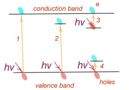
According to the quantum theory, there is a special selection rule, during optical transitions of electrons from one energy band to another. Allowed optical transitions are those when quasimomentum of an electron is constant. These transitions are called direct transitions.
Transitions not allowed by the selection rules are also possible. However, their possibility is lower. The law of conservation of momentum works here, because there are three ‘particles’ that take part in the transition process – electron, photon and phonon. Phonon is the quantum of the oscillation energy of the lattice. Phonon compensates the difference of electron energies in the initial and final states. These transitions are called indirect transitions. In this case excessive momentum transmits to the crystalline lattice. And as far as to make indirect transitions, quasimomentums of three particles should match, this transition has lower possibility than for direct transition.
Exсiton absorption. In some semiconductors during absorption of photons, excitons may appear with special excited electron states of a valence band. Exciton is a system of connected electrons and holes by their intrinsic electrostatic interaction. Energy levels of an excited electron and a hole are usually lower than the bottom of conduction band. It means that exciton energy is less than the forbidden band width.
Exciton can wander across the crystal from one atom to another. Exciton is a neutral combination of electron and a hole. Weak external electromagnetic fields cannot destroy it, or change its trajectory gradually. During collisions with impurity atoms, exciton can break and create two charge carriers, or recombine with the hole and put atoms into a non-excited state. The first will happen if to give an exciton enough energy to move the electron from exciton level to conduction band – with quantity of energy irradiation. This quantity irradiates in the form of phonon usually.
Light absorption by charge carriers. This mechanism of charge carriers from one energy level to another is due to the light quantity in a semiconductor. Charge carriers make oscillations aligned with the electromagnetic field. Accelerating by the field, they collide with the crystalline lattice atoms, giving them kinetic energy. Absorption intensity rises when light wavelength increases.
Light absorption by impurities is due to ionisation or excitation of impurity atoms in the crystalline lattice. For this mechanism light quantity energy wastes when moving electrons from the donor level to conduction band, or from valence band to acceptor level. Impurities ionisation energy is far less than the forbidden band width, impurity absorption of the light is shifted into the infrared field of the spectrum, and can be observed only at low temperatures.
Light absorption by the crystalline lattice is the result of electromagnetic field interaction to an oscillating charge in the crystalline lattice. Lattice absorption is due to the change of oscillation energy of the atoms. It occurs in the infrared part of the spectrum, and is superimposed with impurity absorption and absorption by charge carriers. In Figure 18 the total semiconductor absorption spectrum is shown. There is a gradual fall of the absorption coefficient after intrinsic absorption spectrum part. which is determined by the charge carrier’s concentration in the absorption minimum of the spectrum, hence the dependence on the impurities and temperature. Impurities concentration and its type determines peak position and value of the impurity absorption curve. The coefficient of impurity absorption is usually much smaller then the one for intrinsic absorption, because impurities concentration in the crystalline lattice is much smaller than the concentration of intrinsic semiconductor atoms.
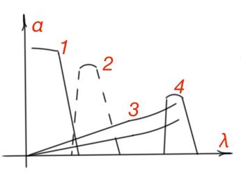
From all the considered mechanisms of optical absorption of semiconductors, only intrinsic and impurity absorption are followed by the charge carrier generation process. Electrical properties of the semiconductor should change due to the optical generation of non-equilibrium charge carriers under the light effect. And these two mechanisms are called photoactive.
Spectral region between intrinsic and lattice absorption is transparent, so pure semiconductors can be used as light filters.
Photoconductivity is a change of electrical conductivity of a semiconductor as a result of electromagnetic irradiation. Photoconductivity is characterised by photon absorption, and this effect is essential for the phenomena. No absorption – no photoconductivity. Only photoactive absorption leads to the conductivity process. And photoconductivity is equal to the difference of a semiconductor’s conductivity in a light environment and a dark one.
Where Δn and Δp are non-equilibrium concentration of charge carriers resulted by optical excitation of semiconductor.
The rate of charge carrier optical generation g0 is determined by the light intensity:
g0 = ŋ0αI, where ŋ0 is a quantum yield of the internal photoelectric effect.
Quantum yield of the internal photoelectric effect is a quantity of charge carrier pairs. In the photoactive part of the spectrum, quantum yield is usually equal to 1, when the energy quantity creates one pair of electron holes.
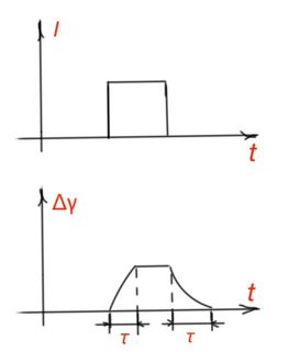
Photoconductivity relaxation. Changing of electrical properties for semiconductors has a temporary nature. After termination radiation, conductivity returns to the value before radiation begun. Knowledge of inertia of photoconductivity helps during electronic component design. Let us consider rectangular light impulse affecting the semiconductor. A decrease or accumulation of non-equilibrium charge carriers determines the difference of generation and recombination rates of charge carriers. Figure 19.
The same formula works for photoconductivity:
When light radiation stops, photoconductivity is determined only by the recombination rate. And steepness of increment and decrement fronts of photoconductivity (Figure 19) depends on the non-equilibrium charge carrier’s life time.
Photoconductivity of a semiconductor depends on the light radiation intensity. After light radiation of a semiconductor, for quite some time, it will reach the stationary value of non-equilibrium charge carrier concentration. For intrinsic absorption:
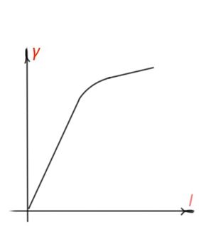
A photoconductivity light intensity graph is shown in Figure 20. Longer charge carrier life time, smaller recombination rate and bigger photoconductivity.
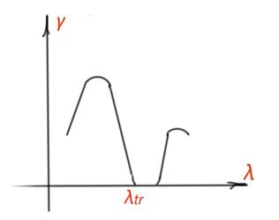
The spectrum photoconductivity curve corresponds to the optic absorption spectra of a semiconductor (Figure 21). Impurity photoconductivity corresponds to the impurity absorption part of the spectra. In the region of large wavelength, photoconductivity is equal to zero, because photon energy is not enough for impurities ionisation. Photoconductivity decrement from the side of short wavelength is a result of resonant character of photoconductivity.
λtr is a trigger value for intrinsic photoconductivity, and corresponds to the intrinsic absorption of a semiconductor. In the region of small λ photons, energies are large, and all recombination processes happen in the thin surface layers of a semiconductor – that’s what we see as a decrement of photoconductivity in Figure 21. Spectrum maximum for intrinsic photoconductivity is determined by the width of the forbidden band for a semiconductor.
Luminescence. Luminescence is a non-heating electromagnetic radiation, with a life time longer then the period of light oscillations. Luminescence should be differentiated from heat solid radiation, processes of light dissipation and reflection, and others. As luminescence is a non-equilibrium process, so the semiconductor should be excited to experience phenomena. During luminescence, the processes of exciting and light radiation are separated in time and space with some intermediate processes. That is why we still can see some light radiation after exciting termination. Compounds, characterised by luminescence phenomena, are called phosphors. Phosphors are usually semiconductors with a wide forbidden band. Depending on the excitation source, phosphors can be divided by three groups:
- Photoluminescence
- Kathodoluminescence
- Electroluminescence
Photoluminescence is a subject of a Stocks-Lumel Law, which states that maximum radiation spectrum is always shifted to the side of a large wavelength in correspondence of absorption spectrum, and some part of the energy dissipating in the semiconductor, transforming in the heating energy. Luminescent properties of solids depend on the defects and impurities in the semiconductor. Impurity atoms, created in the forbidden band of a semiconductor, are responsible for semiconductor luminescence.
In semiconductors, luminescence is due to non-equilibrium charge carrier recombination. There can be a lot more processes before recombination, like charge carrier diffusion, trapping, accelerating by electromagnetic field, etc. Light quantity radiation may occur as a result of interband recombination (from conductance to valence band), excitons recombination, or recombination with the traps. However, not every recombination act is accompanied with light radiation.
Most of the recombination processes in a semiconductor are non-radiant, when energy quantity is transferred to the crystalline lattice. To reach a proper luminescence effectiveness, recombination processes should be under control. Luminescence may occur in a semiconductor with a forbidden band wider then 1.7eV. Some wideband semiconductors have such a high resistance that they can be categorised as insulators. Radiation quantum transition may happen spontaneously and forcibly. During spontaneous transitions, photons emissions do not depend on external factors. Acts of spontaneous radiation occur independently of each other, and spontaneous radiation is non-coherent. Forced quantum transitions occur under the influence of external electromagnetic fields with some exact frequency. Emitting photons and forced radiation have the same frequency, polarisation and phase as a forcing radiation, forced radiation is coherent.
There is two types of electroluminescence. Injecting electroluminescence and prebreakdown luminescence.
#10 Thermoelectrical phenomena and Hall effect in semiconductors


